Introduction
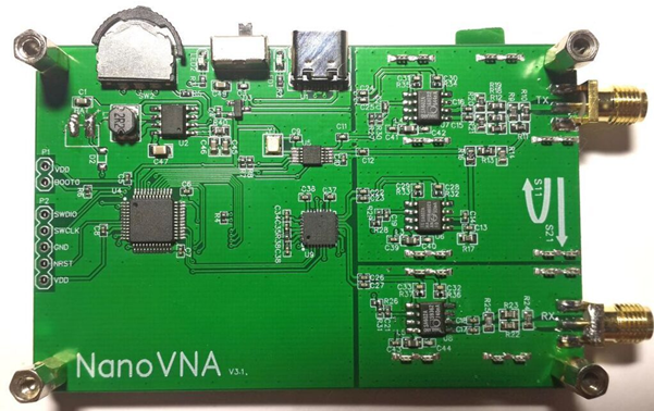
Recently a small vector network analyser (VNA) has become available on the usual auction sites from China. It started life as a kit aimed at hobbyists in China but has evolved into a product that has been widely “cloned” and made available for sale. There are a large number of sellers and apparently several different manufacturers. However at a cost in the £30 to £40 they seemed too good a bargain not to get one! Some of the clones are better than others and it is hard to judge which one you will get when you order one. I bought one from a Chinese seller on Ebay. It was version 3.1 of the PCB and broadly conformed to the boards designed by Hugen79.
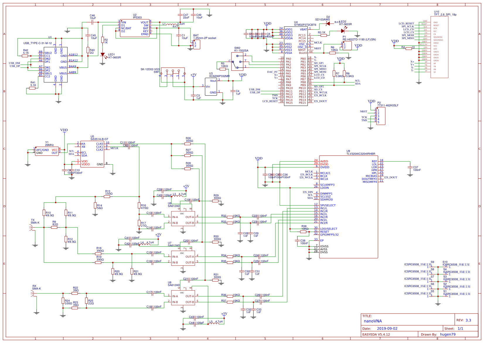
The design makes ingenious use of low cost consumer ICs to produce a VNA that is capable of giving useful results up to 900MHz. The block diagram is below:
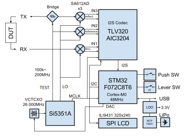
The heart of the unit is an audio codec chip that takes as its inputs the outputs from three SA612 mixers. The mixers are fed with a common local oscillator signal and their outputs are the reflected signal from the DUT, a reference signal and the transmitted signal through the DUT. The mixer inputs are the common local oscillator and:
- The reflected signal sampled by the bridge
- The reference signal
- The transmitted signal from the DUT output
The test signal and the local oscillator are generated by a Si5351A clock generator chip and are spaced by a constant frequency difference in the audio range of 6kHz (or 10kHz with some firmware versions). The three mixer outputs are I and Q signals at a 6kHz (or 10kHz) intermediate frequency, which are digitised in the audio codec chip to provide three data streams to the STM32F Microcontroller which computes the display data to present on the touch screen.
The Si5351A data sheet specifies its maximum output frequency as 200MHz but the designers have found that in practice most of the chips are able to operate to 300 MHz. As the outputs from the clock generator chip are square waves they are rich in odd harmonics and by generating LO and test signals whose third harmonics are spaced by 6 kHz it is possible to extend the frequency range to 900 MHz.
Extending the Frequency Range
Over the past year newer versions of the firmware have appeared on Github and the Nanovna IO group that extend the frequency range of the unit up to 1500 MHz by using the fifth harmonic of the Si5351A output. I was curious to see how well it would work and so I re-flashed the firmware in my unit with the DFU files uploaded to Github by Dislord, [1].
There are extensive guides to flashing firmware to STM32F microcontrollers on the internet and Youtube so I will not cover it here.
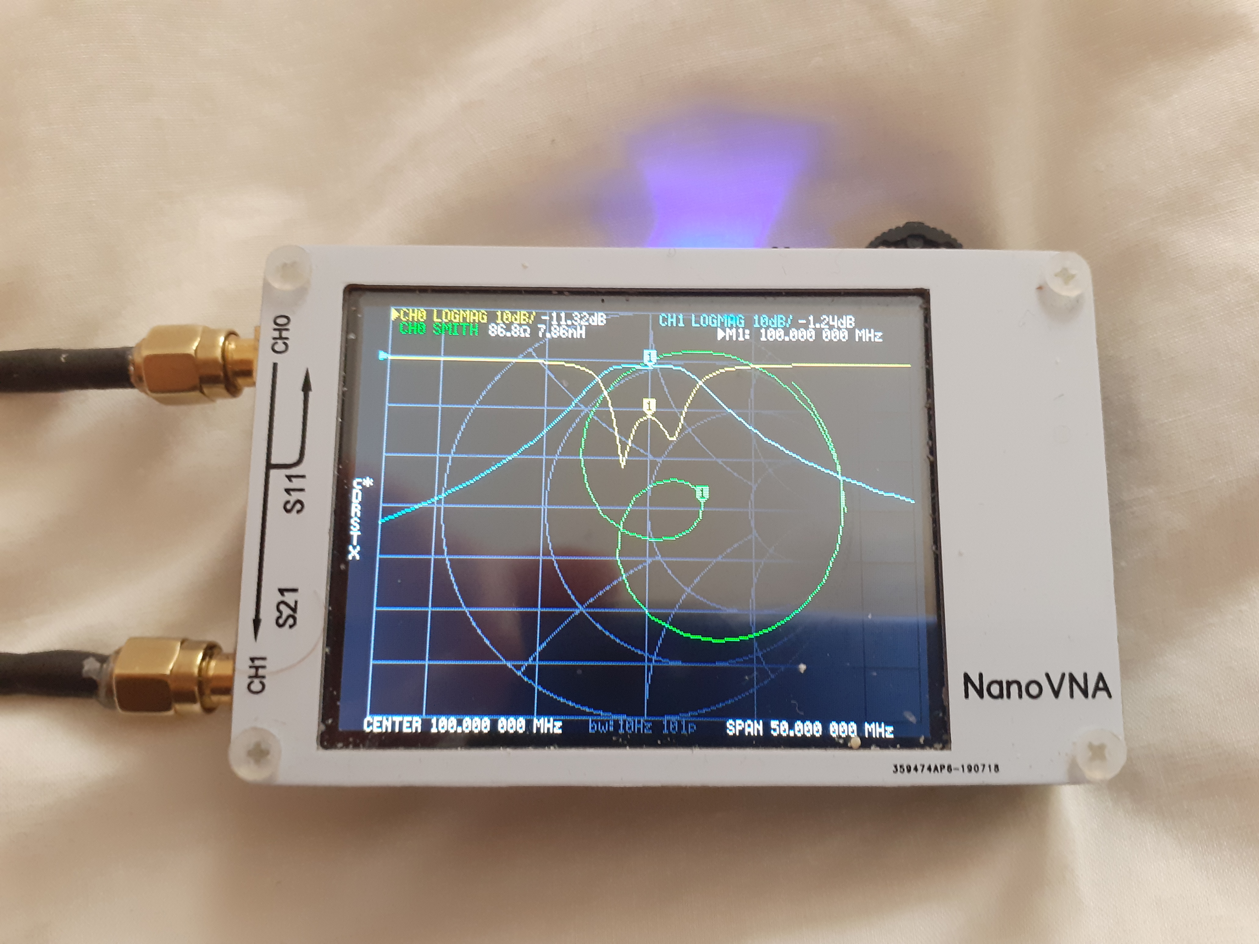
On calibrating my unit set to a span of 100 MHz and a centre frequency of 1300 MHz the results were not encouraging. A 50 ohm load on a Smith chart plot looked a bit like a sizable hedgehog jumping around on the middle of the chart which was not good.
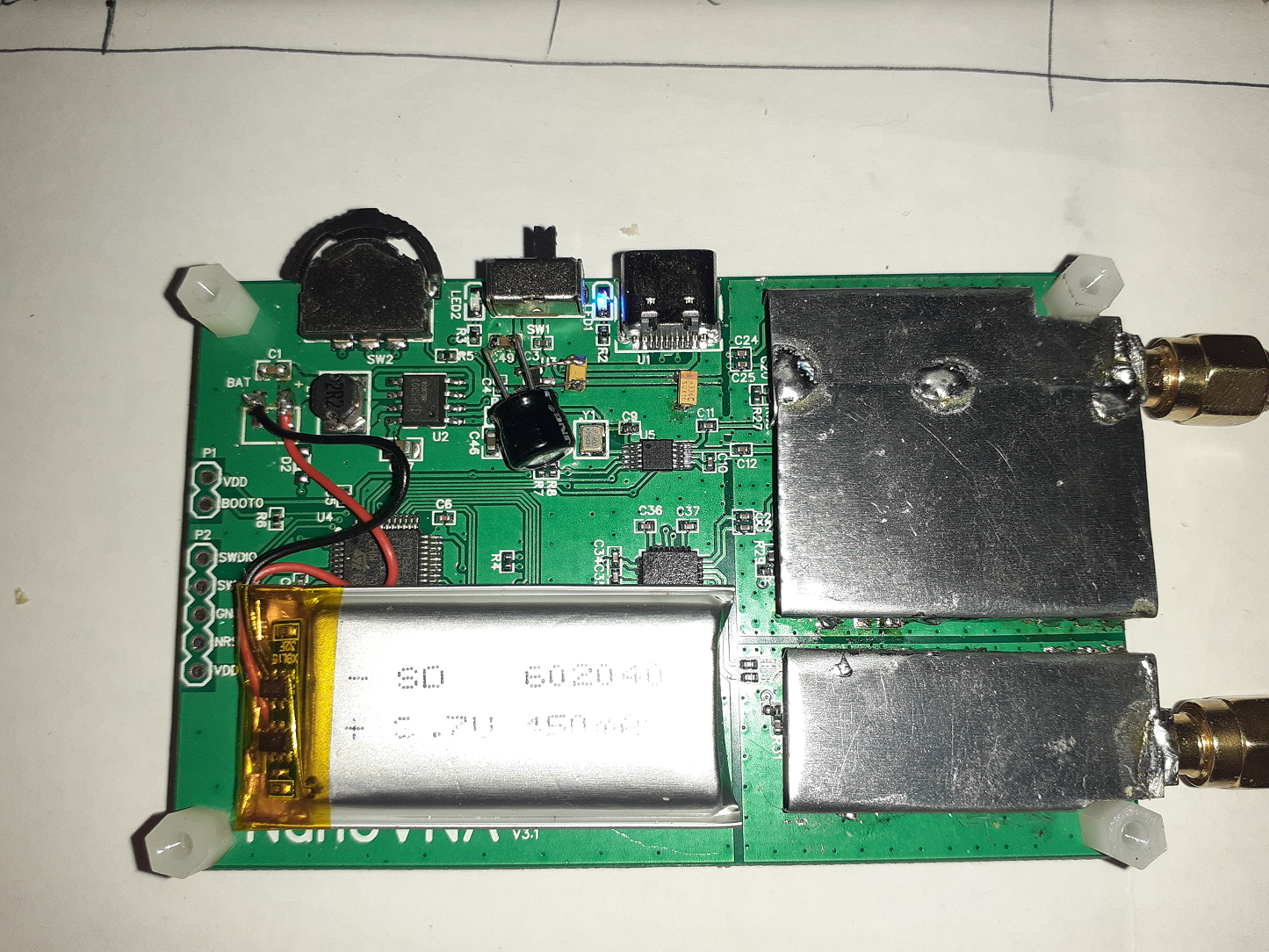
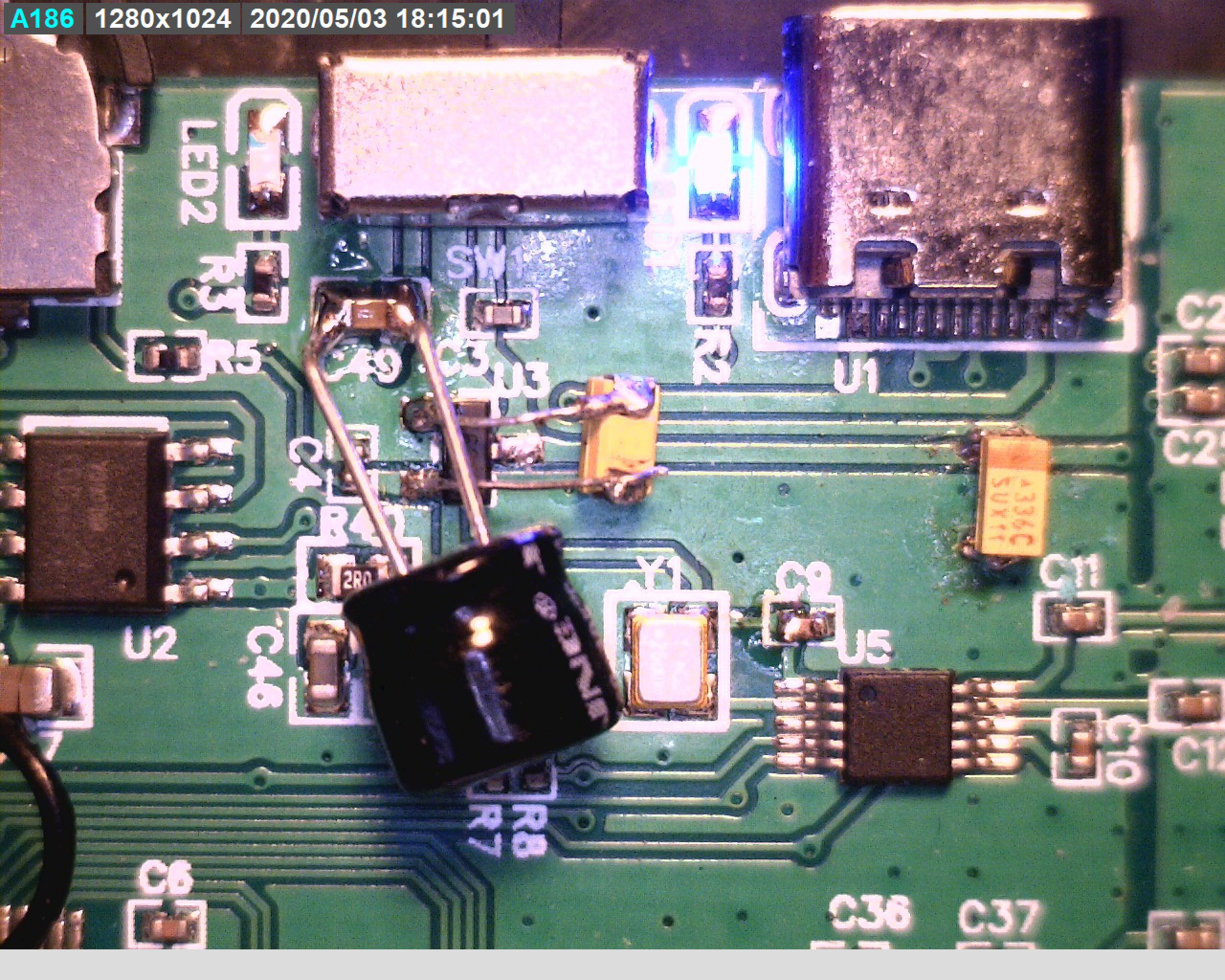
Looking at the schematic revealed that there is a switch mode charge control IC (IP5303) to control the charging of the single cell LiPo battery and also provide the 5 Volt supply when running off the battery. This was a prime suspect as a source of noise. A clue was that the noise was worse when running on battery. Looking at the signal at the CH0 port with a spectrum analyser revealed that it was noisy. Taking the back off the unit and probing with a ‘scope showed that there was noise on the 3V3, VDD rail powering the microcontroller and the Si5153A. Adding a 33uF 16V tantalum SMD capacitor to the 3V3 rail, across C4 on the schematic(link) Vdd rail reduced the noise on the RF signal at the test ports suggesting that the source was switching noise from the IP5303 modulating the Si5153A output. This did not have an immediate effect on the noise on the trace and attention turned to the 5 V rail powering the three SA602/612 mixers. This showed several 10s of mV of noise and two further capacitors were added across this rail. Firstly a 33 uF SMD tantalum type was placed on the track leading to the 3V3 regulator and a 220 uF 10 V electrolytic type was placed across C49 on the 5 V output of the IP5303. The positions of the three capacitors are as shown in the two pictures below:
This was found to reduce the noise on the traces considerably suggesting that it was getting in via the power rails to the mixers. I also added tinplate screens over each of the three mixer channels to improve isolation but overall I did not find this made a significant difference. Overall after the addition of the screens and the extra decoupling the unit I have gave the following performance:
|
50-150 MHz |
400-500MHz |
800-900MHz |
1.2-1.3GHz |
|
|
S21 Dynamic Range |
70dB |
55-60dB |
50dB |
35dB |
|
S11 Dynamic Range |
70dB |
40dB |
30dB |
25dB |
Some Results of Calibration at 1300 MHz
Open
Short
50 Ohm load
S21 through
S21 open
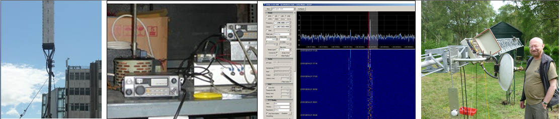
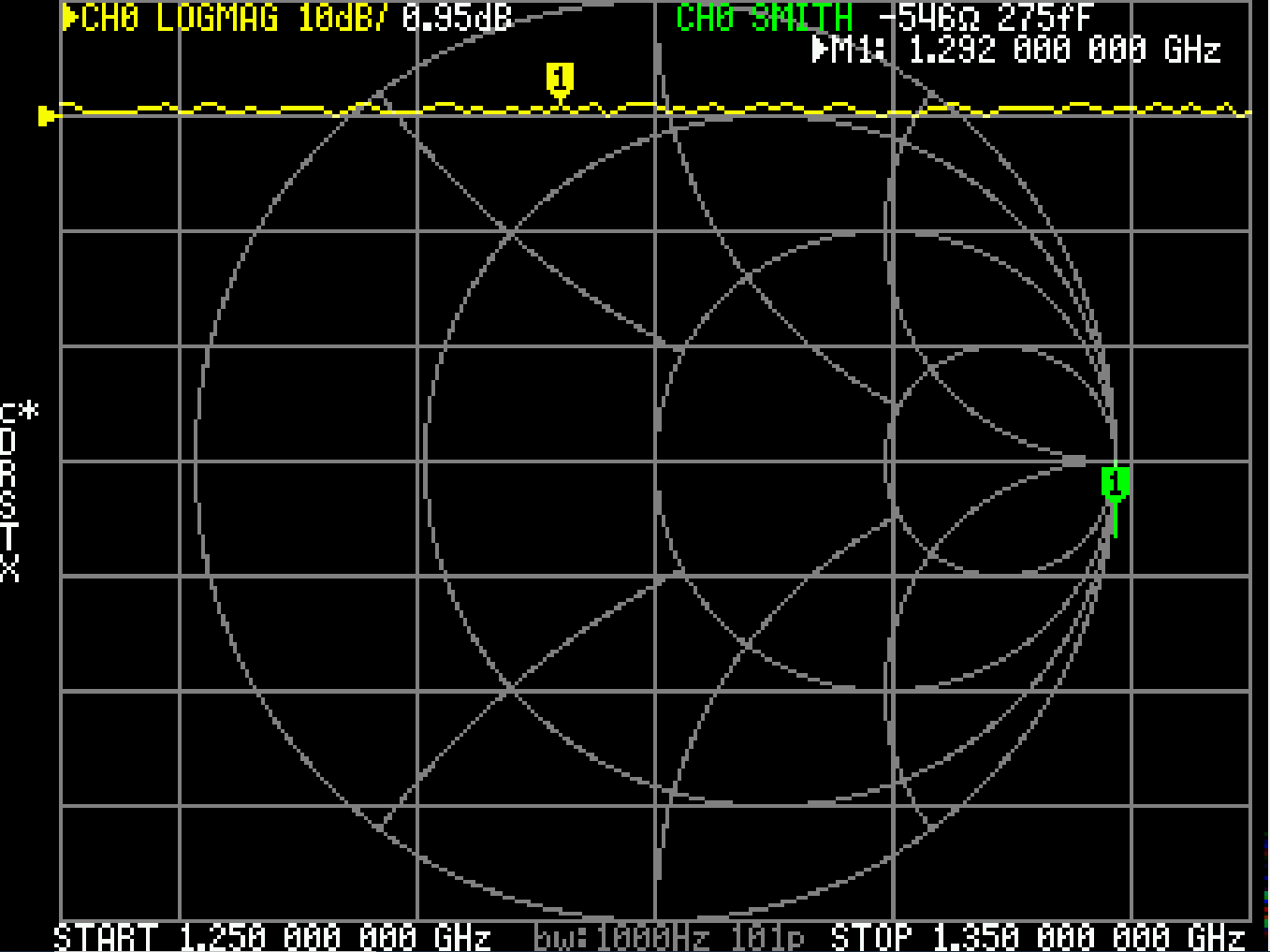
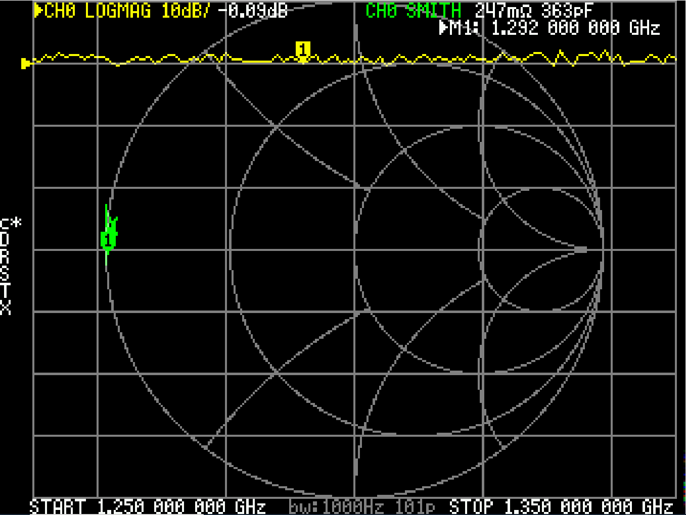
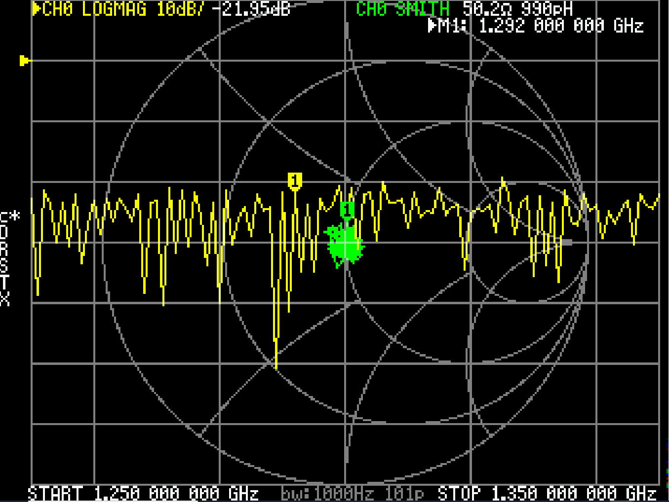
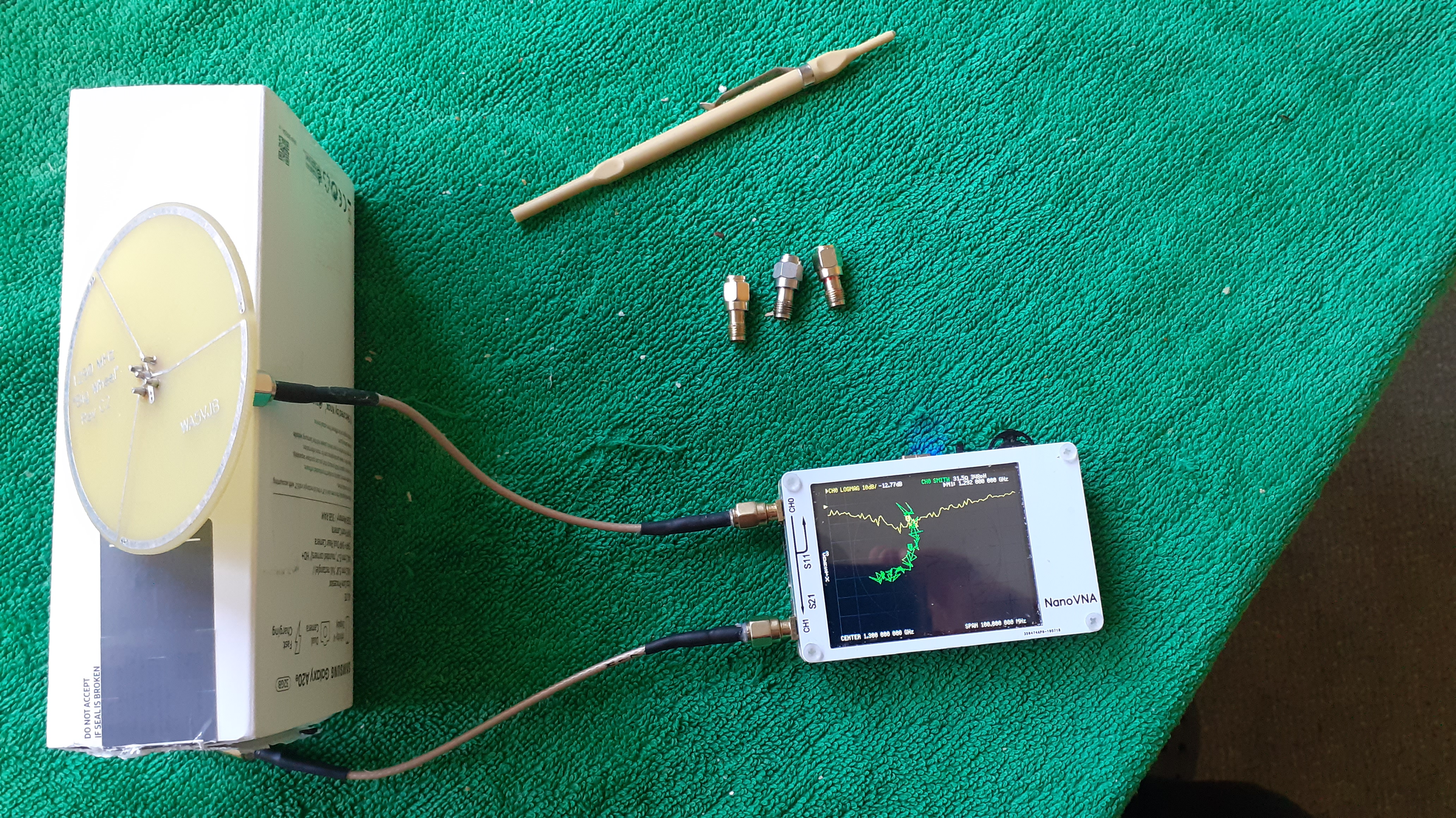
A Simple Reflection Measurement of a 23cm Antenna
The following two pictures show an S11 measurment of a WA5VJB 1290 MHz "Big Wheel" PCB antenna over a frequency range of 1250 MHz to 1350 MHz.
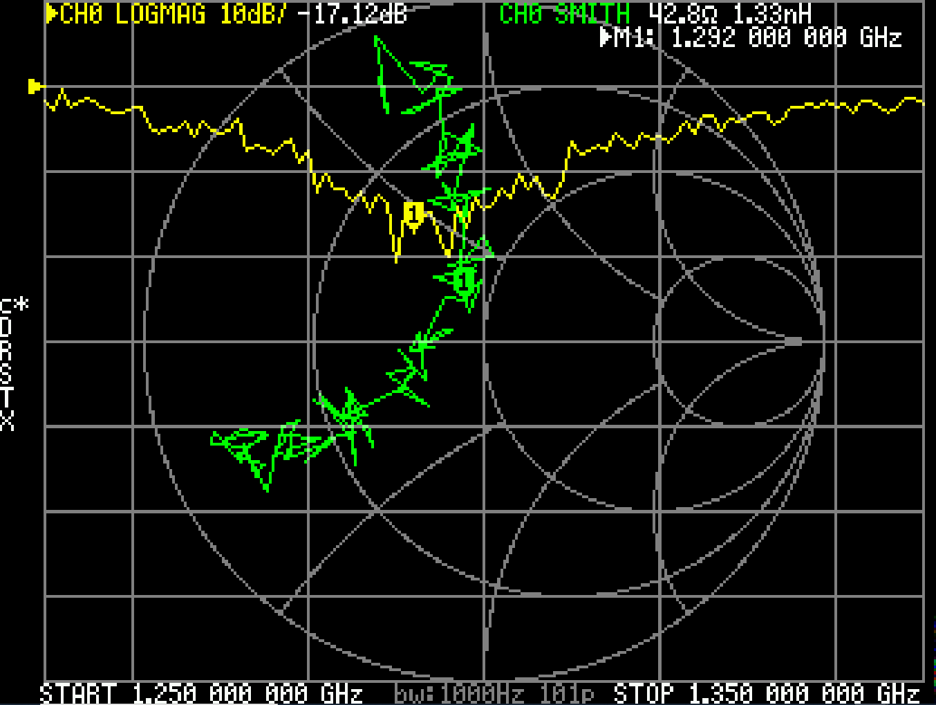
The "Big Wheel"
Conclusion
Overall the unit has become useful as an indicator of performance at frequencies in the 23cm amateur band and the additional capacitors have reduced the noise on the traces at frequencies in its original operating range improving the dynamic range there as well. There may still be some scope for further noise reduction.
Brian Flynn GM8BJF
04 May 2020
References