Introduction
This article presents a versatile PCB design that can be used to provide accurate, stable frequency sources in the frequency range from a few MHz to 4GHz, depending on the components used, with a power output of about +10dBm. It was originally conceived for Microwave applications to replace VHF crystal oscillators that were then multiplied up to the required output frequency, and a number of well-established designs have been published and have served us well, [1]. A number of factors have started to change this, namely, the reduced availability and increasing cost of good quality VHF overtone crystals, the requirement for more accurate frequency setting and the ability to easily change the output frequency when there are changes to our spectrum allocations. These factors start to make the phase-locked-loop (PLL) approach to frequency generation more attractive. There are some aspects of using PLLs which are not so attractive, such as their phase noise performance and their complexity, but in many situations these are outweighed by their advantages. An additional factor is that there are now a number integrated PLL solutions from manufacturers such as Analog Devices (AD) and TI. The object of this article is to present a versatile PCB design that can be used to provide accurate, stable frequency sources in the frequency range from a few MHz to 4 GHz, depending on programming and components used, that gives a power output of around +10 dBm.
PLL integrated circuit architecture
Figure 1 shows a simplified block diagram of a typical PLL integrated circuit. It consists of:
1. A reference divider and latch, the R counter/latch, to divide the reference frequency to the desired phase detector frequency
2. An N divider/latch to divide the VCO frequency to the phase detector frequency
3. A phase detector
4. A charge pump
The VCO and the reference oscillators are external to the integrated circuit. Both of the divider/latches are programmed via a three wire SPI serial data bus. This is used to keep the pin-count on the package to a reasonable level.

Figure1: Simplified block diagram of a typical PLL chip
To build up a complete PLL system with one of these chips, a VCO a reference frequency oscillator, a PLL filter along with some well regulated power supply rails at various voltages must be added as a minimum. It is also necessary to provide some means of programming the R and N counter registers to set the output frequency. This can be done with a Microchip PIC microcontroller. The overall block diagram will then be as shown in Figure 2.

Figure2: Overall PLL block diagram
Detailed Circuit design
The overall circuit is shown in figure 3. The design was for an LO for a 2304 MHz transverter and the LO was to run on 2160 MHz. The PLL chip used is an ADF4113 from AD. To service the PLL chip three different regulated supplies are required, separate 5v digital and analogue rails and around 8v for a mmic ouput amplifier. In addition to the regulators a PIC, a packaged VCO and a reference oscillator are required. The whole PCB is powered from a nominal 12 volt rail.

Figure 3: PLL circuit diagram

Figure 4: PCB layout component placement

Figure 5: Overview of PCB
Component listing
|
C1 |
10n |
0805 |
J1 |
. |
SMA-EINBAUBUCHSE |
|
|
C2 |
100n |
0805 |
J2 |
. |
SMB_EDGE |
|
|
C3 |
1n |
0805 |
J3 |
. |
1X02 |
|
|
C4 |
10n |
0805 |
J4 |
. |
1X02 |
|
|
C5 |
1n |
0805 |
J5 |
. |
SMB_EDGE |
|
|
C6 |
100p |
0805 |
J6 |
. |
SMA-EINBAUBUCHSE |
|
|
C7 |
100n |
0805 |
K1 |
. |
1X03 |
|
|
C8 |
10n |
0805 |
L1 |
. |
1210 |
|
|
C9 |
100nF |
0805 |
L2 |
. |
1210 |
|
|
C10 |
12PF |
0805 |
Q1 |
oscillator_10MHZ |
OSZILLATOR |
|
|
C11 |
1nF |
0805 |
R1 |
18 |
0805 |
|
|
C12 |
10nf |
0805 |
R2 |
18 |
0805 |
|
|
C13 |
PLL_Filter |
0805 |
R3 |
4k7 |
0805 |
|
|
C14 |
PLL_Filter |
0805 |
R4 |
4k7 |
0805 |
|
|
C15 |
PLL_Filter |
0805 |
R5 |
PLL_Filter |
0805 |
|
|
C16 |
1n |
0805 |
R6 |
PLL_Filter |
0805 |
|
|
C17 |
15PF |
0805 |
R7 |
.180 |
0805 |
|
|
C18 |
100n |
0805 |
R8 |
27 |
0805 |
|
|
C19 |
100p |
0805 |
R9 |
180 |
0805 |
|
|
C20 |
22p |
0805 |
R10 |
18 |
0805 |
|
|
C21 |
100n |
0805 |
R11 |
18 |
0805 |
|
|
C22 |
10u |
2817_ELKO |
R12 |
18 |
0805 |
|
|
C23 |
1000p |
0805 |
R13 |
33 |
0805 |
|
|
C24 |
22p |
0805 |
X1 |
CVCO55CL(#1) |
CVCO55CL(#1) |
|
|
C25 |
10n |
0805 |
||||
|
C26 |
100n |
1411_ELKO |
||||
|
IC1 |
. |
SO8_SOT96-1 |
||||
|
IC2 |
. |
SO8_SOT96-1 |
||||
|
IC3 |
. |
DIL8 |
||||
|
IC4 |
IC4 |
TSSOP16 |
||||
|
IC5 |
. |
SO8_SOT96-1 |
||||
|
IC6 |
MAR4 |
MAR4SM(#2) |
||||
Obtaining the PCB design
The PCB design files can be downloaded from this website [2]. The design was done with a package called Target. A trial version of the software, which is adequate for this design, can be downloaded as freeware from the publisher’s website [3] Loading the design file into Target will allow you to preview and edit the design. The design file can be sent to your favourite PCB house to get it made. It is possible output Gerber files from Target, but many PCB houses will accept Target files. I have used two manufacturers PCB-Pool [4] and Jackaltac [5]. Both of these take Target files. The latter is a service aimed at hobbyists and is a low-cost no-frills service. It is possible to panel up the design and get a number of boards made at the one time to spread the cost either with friends or other projects. The components are all surface mount apart from the PIC, the reference oscillator and the connectors. The ICs are in TSSOP packages and are pretty straight forward to solder. (Compared to some other devices!)
Programming frequencies into the PIC microcontroller.
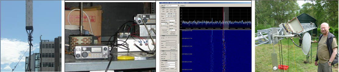
The PCB is designed to take VCOs in a 16-QFN package. This package is widely used for VCOs and it pretty standard. The first step is to obtain a VCO that covers your desired frequency range. The tuning voltage output by the ADF411X chips is 0 – 5 volts. The next step is to decide on the four register latch values that must be programmed into the ADF411X to set it to your desired frequency. For this use the software available from AD [6] called “Integer-N Software”. This can be downloaded from their website and installed in the usual way. It provides a GUI which allows you to specify the reference frequency and the output (VCO) frequency and computes the register values to programme into the PIC. The AD website is an extensive resource and provides a wealth of information on the design of PLLs.
PIC Programme
The assembler code for programming the PIC can be down loaded from [2]. This code was written by John GM8OTI and is well commented. Find the section containing the different register values and edit to enter the values calculated previously. An eight pin DIL packaged PIC was used in the PCB design to allow it to be plugged in and out of the PCB. It is recommended that the PIC is plugged in and out of the PCB. Although I preferred to remove the PIC for programming, the board layout does include a pin header K1 for In Circuit Serial Programming, which may be used if desired (with a suitable adapter lead).
PLL filter design
To choose the values of the components in the PLL filter download the programme called “ADIsimPLL” from the AD website, [6]. This allows you to choose the type of filter you want to use and will give you component values. Tracking is provided on the PCB for different filter orders. The software allows you set different filter bandwidths to optimise the phase noise behaviour.
PCB design options
The PCB has been laid out to be as flexible as possible. Different forms of connector can be used, either through-hole types or edge mount. Connectors can be SMA, SMB or SMC. The Reference oscillator can be omitted and the reference fed externally on a connector. The IC pin-out is very standard across a considerable range of both integer-N and fractional-N PLL chips covering a wide range of frequencies from both AD and other manufacturers. The list in Table 1 shows some of those available, but is not exhaustive.
|
ADF4110 |
550 MHz |
Int-N |
|
ADF4111 |
1200 MHz |
Int-N |
|
ADF4112 |
3000 MHz |
Int-N |
|
ADF4113 |
4000 MHz |
Int-N |
|
ADF4116 |
550 MHz |
Int-N |
|
ADF4117 |
1200 MHz |
Int-N |
|
ADF4118 |
3000 MHz |
Int-N |
|
ADF4153A |
4000 MHz |
Frac-N |
|
ADF4154 |
4000 MHz |
Frac-N |
|
LMX2306 |
550 MHz |
Int-N |
|
LMX2316 |
1200 MHz |
Int-N |
|
LMX2326 |
3000 MHz |
Int-N |
Table 1: A list of the different parts that share the same pin-out.
Parts availability
All of the parts are readily available from most suppliers with the possible exception of the VCO. These are available from Digikey [7] who carry an extensive range and they are often available from sellers on the usual on-line auction sites – just watch the tuning voltage range and the power supply voltage.
Conclusions
This article has presented the design of a flexible PCB layout for a PLL that can be configured for operation at frequencies in the range from a few MHz to 4GHz. The author has used it for an oscillator for a GPS locked 20.480 MHz reference for and FT736R as well as LO for microwave applications at 880 MHz, 2160 MHz and 2556 MHz. The design files are made available others to use as is or to modify to their own requirements.
References
1. Sam Jewell, “Microwave signal source”, Radcom, September 2008, P80-1.
Useful links including PIC and Ardunio code and PCB CAD file
3. http://ibfriedrich.com/index.htm
4. http://www.pcb-pool.com/ppuk/
6. http://www.analog.com/en/index.html