Recently two varieties of PCB have become available from different Chinese internet outlets which have AD ADF5355 PLL ICs on them. They are described as “54MHZ-13.6GHZ RF ADF5355 PLL Phase-locked Loop VCO Synthesizer Board”. One on 1.6 mm FR4 board with green solder resist and the other on a thinner board material which again appears to be FR4 but with black solder resist. Both have broadly similar circuitry on them which closely follows the design of the AD evaluation board for the chip, but there are some differences.

Figure 1. Green PCB

Figure 2. Black PCB
Both boards are available for prices starting at about £55 which is about the one off price for the ADF5535 chip in the UK. They can be made to work under the control of a PC via their SPI bus, [1,2], with the AD evaluation software. I have now had one each type of board to try out and they both functioned correctly but the phase noise was a bit disappointing and the output powers were lower than quoted in the data sheet. The lack of output power is easily overcome with a MMIC amplifier and hardly surprising considering the FR4 substrate, but the PN performance was considerably worse than suggested by the data sheet and merited further investigation. The schematic diagram of the black PCB can be downloaded from here,[3].
Phase noise reduction
My initial hunch was that the power lines were the source of the noise. There are two voltage regulators on the boards, one a LT176333 which powers both the 3.3 Volt analogue and digital Vdd lines and the other a LT17635 which powers the VCO and charge pump circuitry with 5V. This is powered directly from the output of the regulator and there is no further on-chip regulation, whereas the 3.3 V rails are further regulated down to 1.8 V on-chip. Both the LT parts are billed as “low-noise” in the data sheet, but I noted that the AD evaluation PCB design used AD parts which are considerably more expensive than the LT parts. Their respective data sheets reveal that the AD parts were about ten times less noisy. The simple expedient of adding a 3300 uF low ESR capacitor across C30 (on a black PCB) bypasses the noise from the regulator output quite effectively. I used a Rubycon MBZ series 6.3 V part with and ESR of 12 mOhm. The screenshots in figures 3 show the reduction in phase noise at 10 GHz. This also is effective on the green board.


Figure 3. PN before and after addition of Cap across C30 on black PCB.
In order to check whether the chips were now performing as well as they should I measured the PN and compared the result with a simulated PN plot produced by the free ADIsimPLL tool which is provided by AD. The results are shown below.

Figure 4. Measured PN at 10 GHz with the addition of extra decoupling

Figure 5 Simulated PN at 10.4 GHz with a 15 kHz loop bandwidth.
Conclusion
The data sheet does not give PN curves at 10 GHz but does show the behaviour at 5GHz . This suggests that the levels at 100 Hz, 1kHz and 10 kHz should be in the -75 to -80 dBc region which is borne out by the measurements. The conclusion from this is that these boards can be made to realise the full performance of the chips and can be useful RF sources for simple low power beacons, signal generators and local oscillators. They may also be useful for multiplying to the higher bands.
References.
- “PC Control of Analog Devices ADF4XXX Synthesiser chips over USB”, https://gm8bjf.joomla.com/articles/9-pc-control-of-analog-devices-adf4xxx-synthesiser-chips
- ADF5355 evaluation software. http://www.analog.com/en/design-center/evaluation-hardware-and-software/evaluation-boards-kits/eval-adf5355.html#eb-overview
3. ADF5355 schematic for black PCB. http://gm8bjf.joomla.com/images/pdf/ADF5355_sch.pdf
4. ADF4351 schematic for black PCB. http://gm8bjf.joomla.com/images/pdf/ADF4351.pdf
Acknowledgement: Thanks to John Miles KE5FX for making his GPIB Toolkit freely available. This was used to make the various graphs in this article. See: http://www.ke5fx.com/gpib/readme.htm
Addendum 1
Since writing the Scatterpoint article further investigation of the ADF5355 Board and an ADF4351 board has be carried out. This work has concentrated on the “black” PCBs labelled NWDZ. The schematic diagrams of these boards are here [3, 4]. For both boards it was found that adding extra low frequency decoupling the individual power rails gave further small improvements. For the ADF5355 board adding 1000 uF 6.3 V low ESR electrolytic across C29 (AVDD), C31 (DVDD) and C30 (VP5V) gave improved PN. At 12 GHz the PN is around -80dBc 100Hz off the carrier. For the ADF4351 board adding 1000 uF 6.3 V low ESR electrolytic across C30 (AVDD) and C31 (DVDD) gave much improved PN performance.
15/12/2017
Addendum 2
I have refined the PN measuring setup as I concluded that the noise out of the ADF5355 at 12 GHz was close to the PN floor of my HP8566B SA. I am now down converting the output (suitably padded off) by mixing it with the 12.5755 GHz output from a CTI-Herley PLL to 575.5 MHz and measuring the PN at the lower frequency. This means that the SA is operating on the fundamental of its YIG insead of its third harmonic. This drops the PN floor of the system by 20log3 = 9.5 dB which is a useful improvement. The output from tyhe CTI-Herley is much lower noise that the ADF5355. The plot below shows the result.

Blue trace - ADF5355 running with 25 MHz reference frequency doubled to 50 MHz PD frequency, output frequency of 12 GHz and Icp set to 0.3 mA
Pink trace - ADF5355 as above but with an Icp set to 4.8 mA.
Green trace - Elcom DFS1201 running at 11.600 GHz (for comparison)
Red trace - SA 100 MHz reference output to indicate the PN floor.
The close to carrier noise is improved by the higher bandwidth affored by the higher charge pump current value by 20 dB. All the measurements on the ADF5355 were made on a board which had all three power rails decoupled with 1000 uF 6.3 V low ESR capacitors as described in addendum 1 above.
If carefully decoupled and set up correctly these ADF5355 PCBs can give PN performance close to the now unobtainable Elcom DFS units and are useful as LOs for 24 GHz.
22/12/2017
Addendum 3
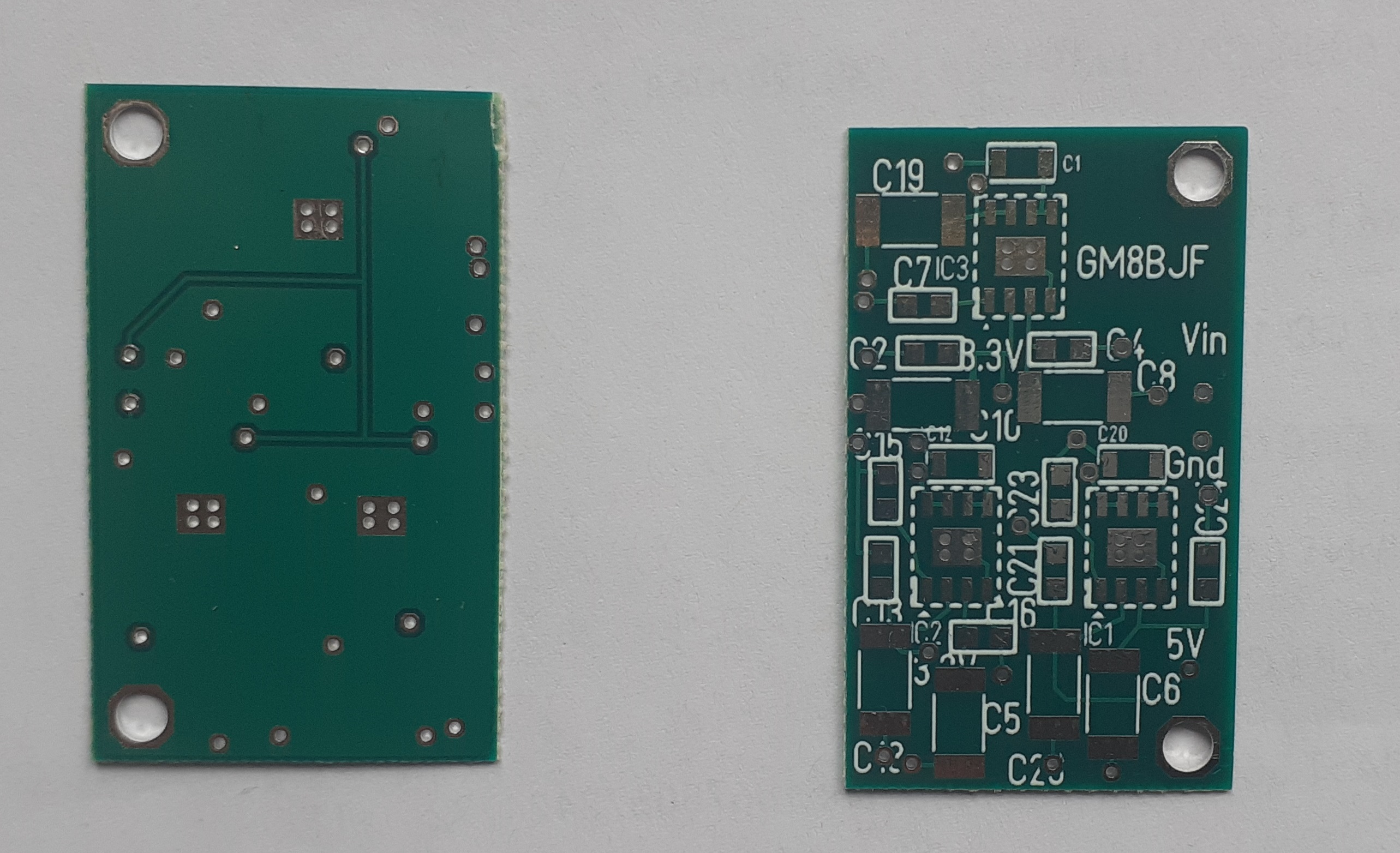
I decided to try using the ADM7150 voltage regulators recommended by AD. As mentioned above they have a noise performance almost ten times better than the LT parts used on the Chinese Evaluation boards. the ADM7150 is a fixed voltage regulator and comes in both 3.3V and 5.0V variants. Unfortunately the pinout is different from the LT1763XX parts on the PCB and they also use the dreaded pin 0 as a ground pad. To use them I decided it was necessary to design a small daughter card to fit over the "Black" board. The layout, schematic and the BoM of the board are below along with a couple of pictures showing the board in place on the original PCB.

PCB Layout

Schematic
| ; | |||||
| Pos | Name | Value | Package | ||
| 1 | C1 | 1uF | 1206 | ||
| 2 | C2 | 10uF | 0805 | ||
| 3 | C4 | 47µF | 2412_ELKO | ||
| 4 | C5 | 47µF | 2412_ELKO | ||
| 5 | C6 | 47µF | 2412_ELKO | ||
| 6 | C7 | 10uF | 0805 | ||
| 7 | C8 | 10uF | 0805 | ||
| 8 | C10 | 47µF | 2412_ELKO | ||
| 9 | C12 | 1uF | 1206 | ||
| 10 | C13 | 10uF | 0805 | ||
| 11 | C15 | 10uF | 0805 | ||
| 12 | C16 | 10uF | 0805 | ||
| 13 | C18 | 47µF | 2412_ELKO | ||
| 14 | C19 | 47µF | 2412_ELKO | ||
| 15 | C20 | 1uF | 1206 | ||
| 16 | C21 | 10uF | 0805 | ||
| 17 | C23 | 10uF | 0805 | ||
| 18 | C24 | 10uF | 0805 | ||
| 19 | C26 | 47µF | 2412_ELKO | ||
| 20 | IC1 | ADM7150ARDZ-5.0 | SOIC127P600X175-9N | ||
| 21 | IC2 | ADM7150ARDZ-3.3 | SOIC127P600X175-9N | ||
| 22 | IC3 | ADM7150ARDZ-3.3 | SOIC127P600X175-9N | ||
Bill of Materials
The PCB CAD programme (Target) can be downloaded here.


The PCB in situ secured on 3mm nuts and pillars
Conclusions: The perfomance of the board was greatly improved over its initial state. It was as good as what was achieved bu adding the physically large electrolytic capacitors described prviously. It does provide a neater, more compact solution. I have some spare PCBs left which I can provide for £5.00 plus postage. These modifications, I believe, get the performance of the board up to what the manufacturer offers in the data sheet. My email address is:
brian dot flynn at tiscali dot co dot uk
PCB Errata 23/08/2018
A couple of errors have come to light on the PCBs I have available. The negative pads of C5 and C23 are not connected to the ground plane. There are nearby ground PTH pads that can be used to make the missing connections.
25/03/2018
PCB Update 24/03/2023
I now have a new batch of PCBs available that have the the two errors mentioned above corrected. These are available on the same basis as the earlier batch as described above.